- 产品详情
- 产品参数
【技术参数】
|
|
|
|
型号
|
AC240TM
|
|
制造厂商
|
Olympus
|
|
探针描述
|
导电探针; 硅基探针;Al反射层; 针尖镀Pt
|
|
类型
|
电学模式
|
|
应用
|
导电模式;静电力模式, 表面电势模式;扫描电容模式;压电力模式;(CAFM; EFM; KPFM; SCM; PFM)
|
【产品详情】
|
悬臂描述
|
|||||

|
Lever
|
1
|
2
|
3
|
4
|
|
|
Spring k (N/m)
|
2 (0.3 - 4.8)
|
-
|
-
|
-
|
|
|
Freq (kHz)
|
70 (45 - 95)
|
-
|
-
|
-
|
|
|
Length (µm)
|
240 (232 - 248)
|
-
|
-
|
-
|
|
|
Width (µm)
|
40 (39 - 41)
|
-
|
-
|
-
|
|
|
Thickness (µm)
|
2.3 (1.6 - 3.0)
|
-
|
-
|
-
|
|
|
Shape
|
rectangular
|
-
|
-
|
-
|
|
|
Material
|
Silicon
|
-
|
-
|
-
|
|
|
Reflex Coating (nm)
|
Al (100)
|
-
|
-
|
-
|
|
针尖描述
|
||

|
Tip radius (nm)
|
28 +/- 10
|
|
|
Tip height (µm)
|
14 +/- 1
|
|
|
Front angle (°)
|
0 +/- 1
|
|
|
Back angle (°)
|
35 +/- 1
|
|
|
Side angle (°)
|
15 +/- 1
|
|
|
Tip shape
|
3-sided
|
|
|
Tip material
|
Silicon
|
|
|
Tip coating (nm)
|
Ti/Pt (5/20)
|
DESCRIPTION
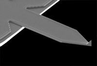
f = 70 kHz | k = 2 N/m | tip coating: Ti/PtEach pack contains 10 probes. The new OMCL-AC240TM type 3 series with ‘New Concept Chip’.Platinum-deposited cantilever is suitable for electrical characterization application such as electric force microscopy (EFM), Kelvin probe force microscopy (KFM).
OUTSTANDING FEATURES:
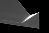
1. Platinum coating for electrical measurementThe platinum layer is deposited on the basic silicon probe with the titanium interfacial layer. The surfaces of precious metal coatings are free from oxidization and are electrically stable. The platinum layer on the probe has smooth surface, and the tip shape follows the shape of the basic silicon probe. Unprecedented probe sharpness of 15 nm (Nom.) in radius as a metal coated probe is worth trying in studying devices.2. The higher conductivity even with a sharper probeOMCL-AC240TM type3 with tip side platinum coating shows higher conductivity while its probe is sharpened more than Olympus conventional product. This probe reveals sample surface precisely both in electrically and in topographically.3. Ideally point terminated probeThe apex of the tetrahedral probe is ideally point terminated. The tetrahedral probe shows good symmetry viewed from the front of the cantilever.4. Acclaimed ‘TipView’ structureThe probe can be easily positioned at the exact point of your interest due to ‘TipView’ structure. The probe is located at the exact end of the cantilever so that the probe apex is not obscured during optical observations.5. Reflex side aluminum coatingThin aluminum film with the thickness of 100 nm is deposited on the cantilever for reflecting light from the deflection sensor in the AFM equipment. High reflex for high S/N sensing can be expected.6. Ease in chip handling: ‘New concept chip’The ideally vertical side-walls of the chip make tweezing easy and eliminate problems with chipping and debris.